
搜索结果: 1-9 共查到“光学工程 lithography”相关记录9条 . 查询时间(0.077 秒)
Bragg-Angle Diffraction in Slant Gratings Fabricated by Single-Beam Interference Lithography
Slant Grating Single-Beam Interference Lithography Bragg-Angle Diffraction
font style='font-size:12px;'>
2013/1/30
A single-beam interference-lithography scheme is demonstrated for the fabrication of large-area slant gratings, which requires exposure of the photoresist thin film spin-coated on a glass plate with p...
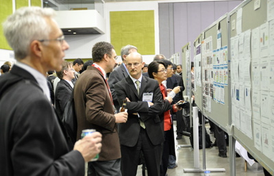
EUV is hot topic at SPIE Advanced Lithography 2011(图)
SPIE EUV Advanced Lithography semiconductor industry
font style='font-size:12px;'>
2011/4/21
First noted in 1965, Moore's law describes the trend of increasing computer technology, which has continued for more than 50 years and is expected to keep going for decades more in the semiconductor i...

Community readies for SPIE Advanced Lithography amidst market growth indicators(图)
SPIE semiconductor industry EUV
font style='font-size:12px;'>
2011/4/22
Bolstered by a record 2010 and continued indicators predicting market growth for the industry, the lithography community is preparing for its annual gathering at SPIE Advanced Lithography. Finding sol...
Directional Photofluidization Lithography for Nanoarchitectures with Controlled Shapes and Sizes
Surface plasmon resonance metallic nanostructures azopolymer directional photofl uidization
font style='font-size:12px;'>
2015/8/10
Highly ordered metallic nanostructures have attracted an increasing interest in nanoscale electronics, photonics, and spectroscopic imaging. However, methods typically used for fabricating metallic na...
Low Loss Chalcogenide Glass Waveguides Fabricated By Thermal Nanoimprint Lithography
Glass waveguides Nonlinear optics integrated optics
font style='font-size:12px;'>
2015/6/5
Low loss thermally nanoimprinted chalcogenide waveguides are demonstrated for the first time,uniquely using a soft PDMS stamp. Losses of 0.24dB/cm at 1550nm limited by Rayleigh scattering were achieve...
Real-time mask-division technique based on DMD digital lithography
digital lithography technique mask-division technique DMD-based lithography edge
font style='font-size:12px;'>
2011/5/6
Digital lithography technique is a promising tool for the fabrication of binary optical element. In
this paper, we present the mask-division technique to improve the lithography quality. A piece of
...
Laser Produced Plasma for EUV Light Source For Lithography
EUV light Laser produced plasma Light source for tin and xenon plasma
font style='font-size:12px;'>
2009/6/8
We describe properties of laser produced plasmas (LPP) for extreme ultra violet (EUV) light source for next generation lithography as an industrial application of LPP. We briefly present three topics ...
Wafer Surface Charge Reversal as a Method of Simplifying Nanosphere Lithography for Reactive Ion Etch Texturing of Solar Cells
Simplifying Nanosphere Lithography Solar Cells
font style='font-size:12px;'>
2008/10/30
A simplified nanosphere lithography process has been developed which allows fast and low-waste maskings of Si surfaces for subsequent reactive ion etching (RIE) texturing. Initially, a positive surfac...
Linewidth control by overexposure in laser lithography
linewidth overexposure laser lithography
font style='font-size:12px;'>
2011/5/5
In micro-electronic and micro-optical manufacturing, especially in the fabrication of linewidth-variation-sensitive devices, we sometimes care getting stable or precise linewidth rather than creating ...