
ЫбЫїНсЙћ: 31-45 ЙВВщЕНЁАЙЄбЇ NanoscaleЁБЯрЙиМЧТМ53Ьѕ . ВщбЏЪБМф(0.062 Уы)
жаЙњПЦбЇдКАыЕМЬхбаОПЫљГЌОЇИёЪвЗЂБэдкЁЖNanoscaleЁЗЕФГЩЙћБЛбЁЮЊЁАШШЕуТлЮФЁБЃЈЭМЃЉ
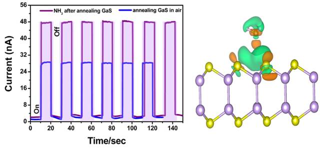
АыЕМЬх ЪЏФЋЯЉ ЖўЮЌВФСЯ Н№ЪєСђЛЏЮя ЖўЮЌGaSГЌБЁАыЕМЬх
font style='font-size:12px;'>
2014/2/18
ЖўЮЌАыЕМЬхВФСЯгЕгаЖРЬиЕФЮяРэаджЪЃЌПЩвдгІгУгкВЛЭЌЕФММЪѕСьгђЃЌвђДЫГЩЮЊСЫФЩУзНЛВцбЇПЦЕФбаОПШШЕуЁЃЪЏФЋЯЉЪЧФПЧАбаОПзюЮЊЙуЗКЕФЖўЮЌВФСЯЃЌЕЋгЩгкЦфДјЯЖЮЊСуЃЌЯожЦСЫЫќдкаэЖрСьгђжаЕФгІгУЁЃзїЮЊЪЏФЋЯЉЕФРрЫЦЮяЃЌОпгаАыЕМЬхДјЯЖЕФН№ЪєСђЛЏЮяБИЪмЙизЂЁЃЛљгкетаЉЖўЮЌАыЕМЬхВФСЯЕФЙтЕчЦїМўОпгагХдНЕФадФмЃЌВЂЧвПЩвдЩшМЦИДдгЕФЦїМўНсЙЙЁЃгЩгкДѓЕФБШБэУцЛ§ЃЌетаЉЖўЮЌВФСЯОпгаКмКУЕФЦјУєДЋИаФмСІЁЃжЦБИетаЉЖўЮЌВФСЯЕФЕЅВуЛђЩйВуНсЙЙгааэЖр...

New hybrid molecules could lead to materials that function at the nanoscaleЃЈЭМЃЉ
New hybrid molecules nanoscale
font style='font-size:12px;'>
2014/3/17
Use your mouse to right-click (Mac users may need to Ctrl-click) the link above and choose the option that will save the file or target to your computer.

Magnetically recoverable, nanoscale-supported heteropoly acid catalyst for green synthesis of biologically active compounds in waterЃЈЭМЃЉ
Core-shell particle Magnetically recoverable catalyst Heteropoly acid Xanthene Hydroacridine
font style='font-size:12px;'>
2013/9/25
12-Tungstophosphoric acid supported on aerosil silica and silica-coated ІУ-Fe2O3 nanoparticles was prepared and characterized using transmission electron microscopy, scanning electron microscopy, and i...
An approach based on particle swarm computation to study the nanoscale DG MOSFET-based circuits
Particle Swarm DG MOSFET Optimization nanoscale compact model
font style='font-size:12px;'>
2010/11/22
The analytical modeling of nanoscale Double-Gate MOSFETs (DG) requires generally several necessary simplifying assumptions to lead to compact expressions of current-voltage characteristics for nanosca...
Mapping local optical densities of states in silicon photonic structures with nanoscale electron spectroscopy
Mapping local optical densities silicon photonic structures nanoscale electron spectroscopy
font style='font-size:12px;'>
2015/8/10
Relativistic electrons in a structured medium generate radiative losses such as Cherenkov and transition radiation that act as a virtual light source, coupling to the photonic densities of states. The...
Microscale and Nanoscale Process Systems Engineering: Challenge and Progress
process systems engineering microchemical engineering nanotechnology
font style='font-size:12px;'>
2009/11/16
This is an overview of the development of process systems engineering (PSE) in a smaller world. Two different spatio-temporal scopes are identified for microscale and nanoscale process systems. The fe...

'Universal' equation describes how materials behave at nanoscaleЃЈЭМЃЉ
'Universal' equation materials nanoscale
font style='font-size:12px;'>
2009/11/24
Understanding how materials behave at tiny length scales is crucial for developing future nanotechnologies and continues to be a great challenge for both theoretical and experimental physicists alike....
Planar Lenses Based on Nanoscale Slit Arrays in a Metallic Film
Planar Lenses Nanoscale Slit Arrays Metallic Film
font style='font-size:12px;'>
2015/8/10
We experimentally demonstrate planar lenses based on nanoscale slit arrays in a metallic film. Our lens structures consist of optically thick gold films with micron-size arrays of closely ...
Metal-dielectric-metal plasmonic waveguide devices for manipulating light at the nanoscale
Metal-dielectric-metal plasmonic waveguide devices nanoscale
font style='font-size:12px;'>
2015/8/10
We review some of the recent advances in the development of subwavelength plasmonic devices for manipulating light at the nanoscale, drawing examples from our own work in metal-dielectric-metal (MDM)p...
Planar metallic;nanoscale slit lenses;angle compensation
Solar energy Nanophotonics photonic crystals
font style='font-size:12px;'>
2015/8/10
We present theoretical considerations as well as detailed numerical design of absorber and emitter for Solar Thermophotovoltaics (STPV) applications. The absorber, consisting of an array of tungsten p...
Planar metallic nanoscale slit lenses for angle compensation
Planar metallic nanoscale slit lenses angle compensation
font style='font-size:12px;'>
2015/8/10
We demonstrate numerically, using a modified total-field/scattered-field formalism, that metallic lenses, based on arrays of nanoscale slits with varying widths in a planar metallic ...
The Weird World of Nanoscale Gold
Weird World Nanoscale Gold
font style='font-size:12px;'>
2009/7/28
Protagonists in the emerging field of nanotechnology
have as their objective the design, construction and
study of useful devices based on nanoscale materials
and objects. Objects or structures tha...
Fault Tolerant Nanoscale Microprocessor Design on Semiconductor Nanowire Grids
Fault tolerance Nanoelectronics Nanofabrics Nanoscale processors Semiconductor nanowires Nanowire grids
font style='font-size:12px;'>
2014/11/7
As CMOS manufacturing technology approaches fundamental limits, researchers are looking for revolutionary technologies beyond the end of the CMOS roadmap. Recent progress on devices, nano-manufacturin...
Extraction, representation and interpretation of nanoscale domain structure information from small-angle scattering patterns
Small-angle scattering synchrotron radiation polymers nanostructure
font style='font-size:12px;'>
2009/2/6
A method for SAXS analysis and its applications to the field of materials science is presented, andcorresponding papers are reviewed. The method permits the topological structure information contained...
Propagating plasmonic mode in nanoscale apertures and its implications for extraordinary transmission
apertures aperture arrays extraordinary transmission Fano interference
font style='font-size:12px;'>
2015/8/10
We studied the interaction of different pathways by which extraordinary transmission through nanoscale aperture arrays arises and obtained a complete physical picture that incorporates both propagati...
жаЙњбаОПЩњНЬг§ХХааАё-Ьѕ
- е§дкМгди...
жаЙњбЇЪѕЦкПЏХХааАё-Ьѕ
- е§дкМгди...
ЪРНчДѓбЇПЦбаЛњЙЙХХааАё-Ьѕ
- е§дкМгди...
жаЙњДѓбЇХХааАё-Ьѕ
- е§дкМгди...
ШЫЁЁЮя-ЦЊ
- е§дкМгди...
ПЮЁЁМў-ЦЊ
- е§дкМгди...
ЪгЬ§зЪСЯ-ЦЊ
- е§дкМгди...
баеазЪСЯ -ЦЊ
- е§дкМгди...
жЊЪЖвЊЮХ-ЦЊ
- е§дкМгди...
ЙњМЪЖЏЬЌ-ЦЊ
- е§дкМгди...
ЛсвщжааФ-ЦЊ
- е§дкМгди...
бЇЪѕжИФЯ-ЦЊ
- е§дкМгди...
бЇЪѕеОЕу-ЦЊ
- е§дкМгди...